As an Amazon Associate, we earn from qualifying purchases.

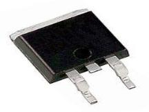
IRFR9310TRLPBF-Vishay-MOSFETs

Gallery

Attributes

Brand name, Manufacturer name, Manufacturer, Attribute02, Brand, MaterialVishay
Attribute00, Attribute01, MPN, Keyword, ModelNumber, Model_number, PartNumber, Part_numberIRFR9310TRLPBF
Attribute03DPAK
Attribute04Vishay Transistors, DPAK Series
Attribute05TO-252
Attribute06P-Channel
Attribute07400 VDC
Attribute081.8 A
Attribute0920 VDC
Attribute103 VDC
Attribute110.1 ?A
Attribute127,000 mOhm
Attribute1311 ns
Attribute1410 ns
Attribute1525 ns
Attribute1624 ns
Attribute17170 ns
Attribute18Yes
Attribute19, Attribute200 lbs
AttributeKey00Manufacturer Part Number
AttributeKey01Item Number
AttributeKey02Manufacturer
AttributeKey03Product Series
AttributeKey04Family Series
AttributeKey05Package
AttributeKey06Circuit Type
AttributeKey07Drain Source Voltage Vds
AttributeKey08Drain Current Id(rms)
AttributeKey09Gate Source Voltage Vgss
AttributeKey10Typ. Vgs(th)
AttributeKey11Gate Leakage Current
AttributeKey12rDS(on)
AttributeKey13Turn On Delay Time
AttributeKey14Rise Time tr
AttributeKey15Turn Off Delay Time
AttributeKey16Fall Time tf
AttributeKey17Trr
AttributeKey18RoHS
AttributeKey19Net Weight
AttributeKey20Gross Weight
CategoryL1Semiconductors
CategoryL2Transistors
CategoryL3, snippetMOSFETs
Extra Product NameIRFR9310TRLPBF-Vishay-MOSFETs
atoms, tierMinQty11
keywordsMOSFETs-Transistors-XSTR
moq, multiple3000
qtyInStock0
SKUIRFR9310TRLPBF-VISH
tierPrice10.69
AdultProduct, Autographed, Memorabilia, TradeInEligibleFalse
AsinB09T5T49KN
ClassificationId306919011
DisplayNameMOSFET
Externally_assigned_product_identifier, Identifier6098000244221
FetchTime1704900199
Height, Width150 75
IdentifierTypeEAN
ItemClassificationBASE_PRODUCT
ItemName, Item_nameVishay IRFR9310TRLPBF, Trans MOSFET P-CH Si 400V 1.8A 3-Pin(2+Tab) DPAK T/R (25 Items)
Item_type_keywordmosfet-transistors
Linkhttps://m.media-amazon.com/images/I/11YgumL9Y5L._SL75_.jpg https://m.media-amazon.com/images/I/11YgumL9Y5L.jpg
Marketplace_idATVPDKIKX0DER
Number_of_items25
ProductTypeELECTRONIC_COMPONENT
Product_descriptionEU RoHS: Compliant with Exemption ECCN (US): EAR99 Part Status: Active HTS: 8541.10.00.80 Automotive: No PPAP: No Product Category: Power MOSFET Material: Si Configuration: Single Channel Mode: Enhancement Channel Type: P Number of Elements per Chip: 1 Maximum Drain Source Voltage (V): 400 Maximum Gate Source Voltage (V): ±20 Maximum Gate Threshold Voltage (V): 4 Operating Junction Temperature (°C): -55 to 150 Maximum Continuous Drain Current (A): 1.8 Maximum Gate Source Leakage Current (nA): 100 Maximum IDSS (uA): 100 Maximum Drain Source Resistance (mOhm): 7000@10V Typical Gate Charge @ Vgs (nC): 13(Max)@10V Typical Gate Charge @ 10V (nC): 13(Max) Typical Gate to Drain Charge (nC): 5(Max) Typical Gate to Source Charge (nC): 3.2(Max) Typical Reverse Recovery Charge (nC): 640 Typical Input Capacitance @ Vds (pF): 270@25V Typical Reverse Transfer Capacitance @ Vds (pF): 8@25V Minimum Gate Threshold Voltage (V): 2 Typical Output Capacitance (pF): 50 Maximum Power Dissipation (mW): 50000 Typical Fall Time (ns): 24 Typical Rise Time (ns): 10 Typical Turn-Off Delay Time (ns): 25 Typical Turn-On Delay Time (ns): 11 Minimum Operating Temperature (°C): -55 Maximum Operating Temperature (°C): 150 Packaging: Tape and Reel Maximum Positive Gate Source Voltage (V): 20 Maximum Pulsed Drain Current @ TC=25°C (A): 7.2 Maximum Junction Ambient Thermal Resistance on PCB (°C/W): 50 Typical Gate Plateau Voltage (V): 5.1 Typical Reverse Recovery Time (ns): 170 Maximum Diode Forward Voltage (V): 4 Supplier Package: DPAK Pin Count: 3 Standard Package Name: TO-252 Mounting: Surface Mount Package Height: 2.39(Max) Package Length: 6.73(Max) Package Width: 6.22(Max) PCB changed: 2 Tab: Tab
Product_site_launch_date2022-02-15T19:37:39.628Z
Typeean
VariantMAIN
WebsiteDisplayGroupbiss_basic_display_on_website
WebsiteDisplayGroupNameBISS Basic

Distributor offers

SellerSKUMOQIn stockMultiplePrices
GalcoIRFR9310TRLPBF-VISH300030001 @ $0.69
TMEIRFR9310TRLPBF11
RadwellIRFR9310TRLPBF11
1SourceIRFR9310TRLPBF11
Digi-Key8120330100010001 @ $1.90, 10 @ $1.71, 100 @ $1.37, 500 @ $1.13, 1000 @ $0.97
Future Electronics112984930003000
iodPartsIRFR9310TRLPBF157521
Win SourceIRFR9310TRLPBF11691
HotendaH182725411
Mouser844-IRFR9310TRLPBF29931 @ $1.19, 10 @ $0.96, 50 @ $0.96, 100 @ $0.74, 1000 @ $0.51, 10000 @ $0.44
AvnetIRFR9310TRLPBF30003000 @ $0.51, 6000 @ $0.48, 12000 @ $0.45, 18000 @ $0.43, 30000 @ $0.42
TTIIRFR9310TRLPBF
Digi-KeyIRFR9310TRLPBF-ND30003000 @ $0.69
Avnet EuropeIRFR9310TRLPBF30003000 @ $0.33, 6000 @ $0.31, 9000 @ $0.29
STLAA.comIRFR9310TRLPBF7200
Abacus TechnologiesIRFR9310TRLPBF6000
Ewing ComponentsIRFR9310TRLPBF39688

Related on Amazon

As an Amazon Associate, we earn from qualifying purchases. (paid link) CERTAIN CONTENT THAT APPEARS ON THIS SITE COMES FROM AMAZON. THIS CONTENT IS PROVIDED 'AS IS' AND IS SUBJECT TO CHANGE OR REMOVAL AT ANY TIME.

Vishay IRFR9310TRLPBF, Trans MOSFET P-CH Si 400V 1.8A 3-Pin(2+Tab) DPAK T/R (25 Items)
Brand: Vishay
EU RoHS: Compliant with Exemption ECCN (US): EAR99 Part Status: Active HTS: 8541.10.00.80 Automotive: No PPAP: No Product Category: Power MOSFET Material: Si Configuration: Single Channel Mode: Enhancement Channel Type: P Number of Elements per Chip: 1 Maximum Drain Source Voltage (V): 400 Maximum Gate Source Voltage (V): ±20 Maximum Gate Threshold Voltage (V): 4 Operating Junction Temperature (°C): -55 to 150 Maximum Continuous Drain Current (A): 1.8 Maximum Gate Source Leakage Current (nA): 100 Maximum IDSS (uA): 100 Maximum Drain Source Resistance (mOhm): 7000@10V Typical Gate Charge @ Vgs (nC): 13(Max)@10V Typical Gate Charge @ 10V (nC): 13(Max) Typical Gate to Drain Charge (nC): 5(Max) Typical Gate to Source Charge (nC): 3.2(Max) Typical Reverse Recovery Charge (nC): 640 Typical Input Capacitance @ Vds (pF): 270@25V Typical Reverse Transfer Capacitance @ Vds (pF): 8@25V Minimum Gate Threshold Voltage (V): 2 Typical Output Capacitance (pF): 50 Maximum Power Dissipation (mW): 50000 Typical Fall Time (ns): 24 Typical Rise Time (ns): 10 Typical Turn-Off Delay Time (ns): 25 Typical Turn-On Delay Time (ns): 11 Minimum Operating Temperature (°C): -55 Maximum Operating Temperature (°C): 150 Packaging: Tape and Reel Maximum Positive Gate Source Voltage (V): 20 Maximum Pulsed Drain Current @ TC=25°C (A): 7.2 Maximum Junction Ambient Thermal Resistance on PCB (°C/W): 50 Typical Gate Plateau Voltage (V): 5.1 Typical Reverse Recovery Time (ns): 170 Maximum Diode Forward Voltage (V): 4 Supplier Package: DPAK Pin Count: 3 Standard Package Name: TO-252 Mounting: Surface Mount Package Height: 2.39(Max) Package Length: 6.73(Max) Package Width: 6.22(Max) PCB changed: 2 Tab: Tab
View on Amazon (paid link)