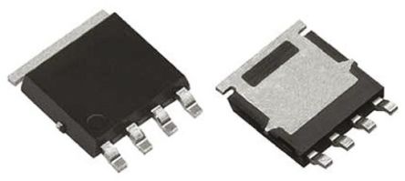
VISHAY SIJ482DP-T1-GE3 | Transistor: N-MOSFET
Attributes
Distributor offers
| Seller | SKU | MOQ | In stock | Multiple | Prices |
|---|---|---|---|---|---|
| TME | SIJ482DP-T1-GE3 | 3000 | 3000 | 3000 @ $1.13 | |
 RS Delivers RS Delivers | 787-9317 | 1 | 1 | ||
| AmazonSC | B00LWM63A6 | 1 | 1 | ||
| Future Electronics | 4025156 | 3000 | 3000 | 3000 @ $0.81 | |
| 78-SIJ482DP-T1-GE3 | 1026 | 1 @ $1.80, 10 @ $1.45, 50 @ $1.45, 100 @ $1.16, 1000 @ $0.84, 10000 @ $0.69 | |||
| SIJ482DP-T1-GE3 | 3000 | 3000 @ $0.83 | |||
| SIJ482DP-T1-GE3 | |||||
| 2283671 | 1 | 1 @ $1.14, 25 @ $0.98, 100 @ $0.89, 250 @ $0.81, 500 @ $0.67 | |||
| 7879317 | 2015 | ||||
| SIJ482DP-T1-GE3 | 3000 | 3000 @ $0.86, 6000 @ $0.80 |
Related on Amazon
As an Amazon Associate, we earn from qualifying purchases. (paid link) CERTAIN CONTENT THAT APPEARS ON THIS SITE COMES FROM AMAZON. THIS CONTENT IS PROVIDED 'AS IS' AND IS SUBJECT TO CHANGE OR REMOVAL AT ANY TIME.
Vishay SIJ482DP-T1-GE3, Trans MOSFET N-CH 80V 60A 5-Pin(4+Tab) PowerPAK SO EP T/R (25 Items)
Brand: Vishay
EU RoHS: Compliant ECCN (US): EAR99 Part Status: Active HTS: 8541.29.00.95 Automotive: No PPAP: No Product Category: Power MOSFET Configuration: Single Triple Source Process Technology: TrenchFET Channel Mode: Enhancement Channel Type: N Number of Elements per Chip: 1 Maximum Drain Source Voltage (V): 80 Maximum Gate Source Voltage (V): ±20 Maximum Gate Threshold Voltage (V): 2.7 Maximum Continuous Drain Current (A): 60 Maximum Gate Source Leakage Current (nA): 100 Maximum IDSS (uA): 1 Maximum Drain Source Resistance (mOhm): 6.2@10V Typical Gate Charge @ Vgs (nC): 24@4.5V|36.5@7.5V|47@10V Typical Gate Charge @ 10V (nC): 47 Typical Input Capacitance @ Vds (pF): 2425@40V Maximum Power Dissipation (mW): 5000 Typical Fall Time (ns): 9 Typical Rise Time (ns): 11 Typical Turn-Off Delay Time (ns): 36 Typical Turn-On Delay Time (ns): 14 Minimum Operating Temperature (°C): -55 Maximum Operating Temperature (°C): 150 Packaging: Tape and Reel Maximum Positive Gate Source Voltage (V): 20 Maximum Continuous Drain Current on PCB @ TC=25°C (A): 21.1 Maximum Power Dissipation on PCB @ TC=25°C (W): 5 Maximum Junction Ambient Thermal Resistance on PCB (°C/W): 65 Typical Diode Forward Voltage (V): 0.73 Typical Gate Plateau Voltage (V): 2.9 Typical Reverse Recovery Time (ns): 46 Maximum Diode Forward Voltage (V): 1.1 Minimum Gate Resistance (Ohm): 0.4 Maximum Gate Resistance (Ohm): 2.2 Supplier Package: PowerPAK SO EP Pin Count: 5 Standard Package Name: SOP Mounting: Surface Mount Package Height: 1.07 Package Length: 4.9 Package Width: 4.37 PCB changed: 4 Tab: Tab Lead Shape: Gull-wing